Elemental Analysis of Thin Films & Coatings
Chemical Identification
Chemical Identification
There are numerous methods to chemically identify films and coatings using FTIR spectroscopy. These are transmittance, attenuated total reflection (ATR), gracing angle reflectance (GIR) or infrared reflection absorption spectroscopy (IRRAS), polarization modulated IRRAS (PMIRRAS). Depending on the film thickness, optical property and supporting substrates different measurement mode(s) can be preferentially applied.

Metallic Coating
Analyze Metallic Coatings

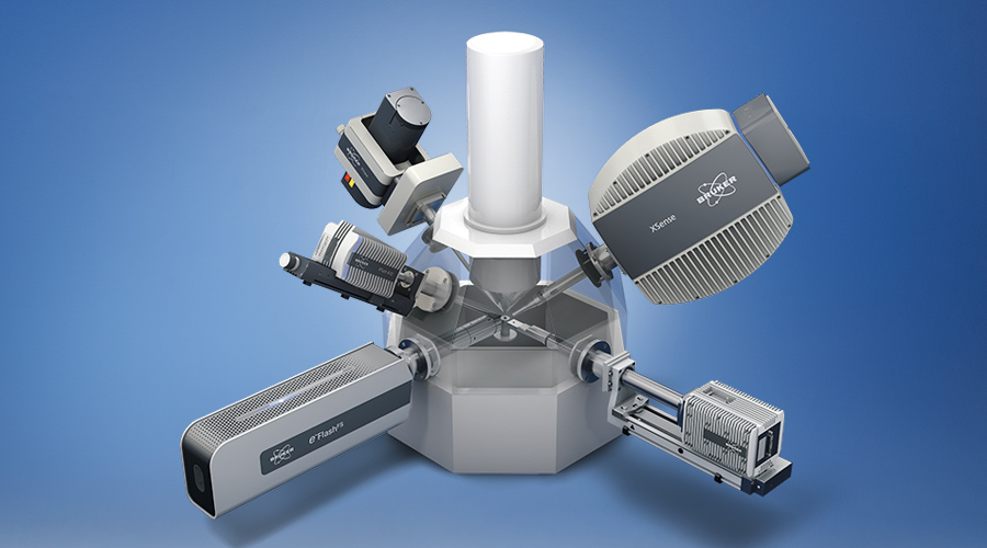
Metallic coatings are used as environmental barriers, actively protecting an underlying material from degradation. In engineering and construction materials they are applied on structural metals and alloys. For optical devices, they are used as mirrors and silvering in headlight reflectors. Metallic coatings are also found in everyday objects such as eyeglasses, utensils, watches, jewelry and toys. The properties of these coatings largely depend on their thickness, crystalline structure, chemical composition and mechanical endurance. Bruker offers a wide range of analytical tools for electron microscopy or as standalone to facilitate the development of such coatings. For example withmicro-XRFfor quantitative analysis of metallic multilayer stacks for composition and coating thickness. And电子显微镜分析仪(EDS,EBSD,WDS)for fast and reliable quantitative chemical and structural anaysis.
Nanostructured Thin Films
Quantitative Characterization of Nanostructured Thin Films with On-axis TKD
Nanomaterials are usually investigated in the Transmission Electron Microscope (TEM). However, it is possible to characterize nanomaterials quantitatively by benifiting from the large field of view of the Scanning Electron Microscope (SEM). Theon-axis TKD为此目标开发了技术;现在,它是使用EBSD硬件在纳米级上产生方向分布测量的良好基于SEM的方法。在此应用示例中,用黄金和白金薄膜的方向分布测量e-Flash FSdetector retroffited withOptimus TKDhead in a FEG-SEM. High speed TKD measurement are achieved at low probe current (<3 nA) allowing to overcome beam drift and achieve ultra high spatial resolution: in 20 minutes over 1000 grains were measured with the smallest grain size being 20 nm and ultrafine features such as twin boundaries were resolved (3nm).